Passive components are an essential part of any electronic system. The manufacturing processes and materials of printed electronics enable the manufacturing of various passive components such as stretchable or bendable conductors, inductors, capacitors, and resistors. This article describes the manufacturing methods of passive components: what type of special materials are used and what kind of functionalities with printed passive components can be achieved. The utilization of printed electronics processes in the manufacturing of passive components enables the use of different substrate materials, considering the requirements of sustainability and a greener future as well as more cost-effective mass manufacturing compared to manufacturing processes of conventional electronics.
Printed electronics refers to the printing of functional materials on different substrates using traditional printing methods, which in many cases has long been used for example in the graphic industry. Substrates to which the printed electronics are manufactured are usually stretchable, bendable, and thin and they are made of plastic, fabric, or fiber-based materials. Printed electronics components and structures easily blend into a wide variety of devices and structures, even following their complex 3D-surfaces and shapes. It brings new possibilities for the manufacturing and development of electronic components and devices. Please see the article “Printed electronics as an enabling technology − introduction to printed electronics” [1] for more information.
Passive components are an essential functional part of any electronic system and application. This article presents an answer to the following questions:
- What kind of functional passive components can be produced by printing?
- What kind of manufacturing methods can be used to make these components and why?
- What kind of materials are needed to manufacture components by printing?
What type of printed passive components are there?
Printed conductors such as flexible metal conductors and transparent conductors, capacitors, resistors, inductors, and antennas are some common examples of functional printed passive components. These passive components are in many cases used together with functional printed active components, such as printed transistors, memory, displays and signage, energy harvesting and storage, printed battery, printed sensors, etc., as a part of a bigger system.
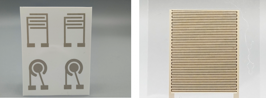
Printed passive components are built on different substrates by adding suitable functional material layer by layer to create the needed functionality. The basic functionality is created in the simplest cases using just conductive material. Slightly more complex structures need also dielectric to separate the conductive parts. Image 1 presents a simple one-layer structure of a touch switch and an example of interdigital capacitor structure. Often passive component functionality and performance are highly dependent on the geometry of the structure [2].
In the following section of this article, we present in more detail two common printed passive components including their functionality, possible manufacturing methods, and needed materials to manufacture them.
Printed conductors, base of electronics system
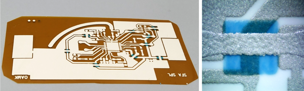
The printed conductor, which is fabricated using almost any additive method, is the base of basically any printed electronics system. Printed conductor inks are broadly available for manufacturing onto different substrates using printing technologies. These materials enable high-yield and high-capacity manufacturing. Printed conductors have usually been utilized in transferring power and signals, antenna structures (explained in more detail in the next paragraph), wirings in general, and in user interfaces. The printed conductor is also a structure that enables the creation of resistive touch screens and heating elements on some surfaces. For most printed electronics systems, the printed circuit board (PCB) constructions are practically used, which makes possible easier embedding and manufacturing of other passive components in the same production processes. Using widely available conductive inks and pastes, printed conductors are manufactured with several different types of printing methods depending on requirements. Because of the high layer thickness requirements of the printed conductors, the screen-printing method, either flatbed or rotary, is commonly applied. This method brings low sheet resistances and thus good conductivity. [3]
Image 2 shows an example of flatbed screen printed conductors on a thin film.
Flexographic or gravure printing is considered when thinner layers than screen-printed layers are needed. The specific need for thinner layers might come in handy in such cases as stacked structures in organic photovoltaic or other active components containing multiple thin layers. Because of lower material consumption, flexographic or gravure printed conductors are also more cost-efficient compared to rotary screen-printed conductors. Digital printing methods such as inkjet and dispensing methods are good choices when only short connections and so-called last-step connections are made through a point-to-point approach.
The materials needed to create printed conductors are mainly silver as a metal particle ink. Copper, gold, and aluminum as functional parts, in the form of micro or nanoparticles, are also available as metal particle inks. Particle-free metal ink is another option that might be successful in the future [4]. Sometimes some metal mixtures and carbon-based graphite or graphene materials are used to reduce cost, sacrificing the performance of the printed conductors. Conductive polymers are used in manufacturing printed conductors in special cases, for example, when optical properties are needed, or electrical properties should be tunable [5]. These special cases where optical properties, mainly transparency, is needed are for example photovoltaic, OLEDs, and touch screen. Despite its undesirable properties, Indium Tin Oxide (ITO) is still the most common transparent conductor material [6].
Printed antennas, vital elements of communication
An antenna converts the energy of the signal-carrying electromagnetic (EM) wave to an electrical signal (current) or electrical signal to an EM wave depending on the reception or the transmission mode in radio engineering. Antenna designs can be omnidirectional or directional. Omnidirectional antennas can transmit or receive radio signals from all horizontal directions simultaneously. Directional antennas are designed in such a way that they transmit or receive signals from a certain direction only.
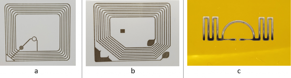
The antenna is one of the vital elements for all radio- and telecommunication devices, including also printed and hybrid structures. Printed antennas are becoming a good option in cases where cost efficiency is a key factor, when small and thin, conformal antennas are essential, and when the antenna is needed to be integrated into structures. Image 3 displays a printed planar square loop wire antenna and a dipole-shaped tag antenna. Wire antennas are usually resonant structures.
Printed antennas can be manufactured using several methods: screen printing, gravure, dispensing, inkjet, and aerosol-jet printing methods have been applied for antenna manufacturing. Sometimes additional printed dielectric layers are required to be printed for interconnections in some antenna designs. The fabrication processes of printed antennas are relatively simple because of the simplicity of usual antenna structures (just a conductor with specific dimensions and electrical properties) and reasonable requirements for dimensions.
Materials for printed antennas are usually the same as for printed conductors. The electric permittivity (ε), material conductivity (σ), loss tangent (tanδ), and permeability (μ) are the specific material parameters in the context of antennas. Traditionally, PCBs are used as the printed antenna’s substrate material. In printed electronics, polymer-based substrates e.g. PET (Polyethylene Terephthalate) and PI (polyimide) are used in printed antennas since those materials are commonly used in printed electronic structures. Paper and glass have also been used as alternative substrate materials. Depending on the required antenna properties, the substrate thickness and surface roughness are crucial to be controlled to reach those properties. [7]
The printed antennas are typically silver (Ag) based. Various types of micro- and nanoparticle-based inks and pastes are utilized based on the applied printing method. The high-quality printed metal inks show conductivity in the range of 50–70 percent bulk silver [8]. Though the manufacturing costs and performances are not competitive with silver copper, gold, and carbon nanotubes have also been considered as the material for the printed antennas in some cases. Since the curing process determines the formation of the microstructure in the metallic structure, this process can make a big difference in antenna properties and performance.
Printed passive components – conclusions
Printing of passive components using the latest functional materials and suitable manufacturing methods is possible with high yield and excellent quality. Commonly used methods of manufacturing printed passive components include screen printing (flatbed or rotary), gravure, flexography, inkjet, and dispensing. Materials used to manufacture printed passive components are most commonly micro- or nanoparticle silver inks, but also copper, gold, and carbon-based inks are used. Conductive polymers are used in special cases when, for example optical properties are needed or electrical properties should be tunable. In the future, it is most likely that novel particle-free inks will be used and the performance of the currently used inks will increase and get closer and closer to bulk metal conductivity.
Harri Määttä
Senior Lecturer
RDI/Digital Solutions
Oulun University of Applied Sciences
Tomi Tuomaala
RDI-Specialist
Centria University of Applied Sciences
If you need more info on printed passive components, or if you are trying to source a possibility to get printed passive components manufactured, please contact Oamk’s PrinLab team, at www.oamk.fi/prinlab
References
[1] Määttä, H., Nissinen, M., Torniainen, N., & Tuomaala, T. (2022). Printed electronics as an enabling technology ‒ introduction to printed electronics. Oamk Journal, (212). Oulun ammattikorkeakoulu. https://urn.fi/URN:NBN:fi-fe2022122173081
[2] Xu, Z. (2022). Creating a CAD Library for Printed Passive Components [Master’s Thesis, Oulu University of Applied Sciences]. Theseus. https://urn.fi/URN:NBN:fi:amk-202205129023
[3] Huttunen, O-H., & Jansson, E. (2019). Printed Conductors. In S. Rousu, K. Särkijärvi & D. Prescott (toim.), Introduction to Printed Intelligence. Handbook for technology training and coaching, 113–116. https://irp.cdn-website.com/88d5bf31/files/uploaded/PrintoCent-Introduction%20to%20printed%20intelligence%20handbook.pdf
[4] Dyson, M. (10.3.2021). Particle-Free Conductive Inks: An Advantageous Alternative? IDTechEx. https://www.idtechex.com/en/research-article/particle-free-conductive-inks-an-advantageous-alternative/23215
[5] Namsheer, K., & Chandra, S. (2021). Conducting polymers: a comprehensive review of recent advances in synthesis, properties, and applications. RSC Advances, 11(10), 5659–5697. https://doi.org/10.1039/D0RA07800J
[6] Vilkman, M. (2019). Transparent conductors. In S. Rousu, K. Särkijärvi & D. Prescott (toim.), Introduction to Printed Intelligence. Handbook for technology training and coaching, 123–129. https://irp.cdn-website.com/88d5bf31/files/uploaded/PrintoCent-Introduction%20to%20printed%20intelligence%20handbook.pdf
[7] Fabritius, T. (2019). Antennas. In S. Rousu, K. Särkijärvi & D. Prescott (toim.), Introduction to Printed Intelligence. Handbook for technology training and coaching, 134–137. https://irp.cdn-website.com/88d5bf31/files/uploaded/PrintoCent-Introduction%20to%20printed%20intelligence%20handbook.pdf
[8] Ivanišević, I., Kassal, P., Milinković, A., Rogina, A., & Milardović, S. (2019). Combined Chemical and Thermal Sintering for High Conductivity Inkjet-printed Silver Nanoink on Flexible Substrates. Biochemical Engineering Quarterly, 33(3), 377–384. http://dx.doi.org/10.15255/CABEQ.2019.1585

Vastaa
Sinun täytyy kirjautua sisään kommentoidaksesi.